I was working on a personal project in the UWM Makerspace the other day, when Chris Beimborn, the Outreach Coordinater of the College of Engineering and Applied Science (CEAS), as well as the leader of a program called EnQuest, an Engineering program for high school age girls.
Over the past semester, they have been working on assembling Solar Panel stands and wiring up some cellphone charger boards for a project for a village in Guatemala. This mountainous village has no electricity, since the power lines were cut during a civil war. However, they still have a need for electricity, and cell phones for internet access. The area has cell phone reception, just no electricity. This is their means for communication with the world.
So, EnQuest was assembling these boards for the solar phone chargers, so villagers wouldn’t have to walk to the next village over to charge their phones. These chargers were then to be brought over by the UWM chapter of Engineering without Borders.
So, Chris comes to me asking if I could take a look at some boards. The boards were shipping out the next day, about about 10 of them weren’t working properly, as well as 2 solar panel assemblies. The SMD work was done by a group of volunteers who weren’t able to repair them in time, so I decided to take a look.
First I started with the datasheet of the only IC on the board, the TPS5516. Looking at the recommended schematic, I drew it out on a whiteboard. 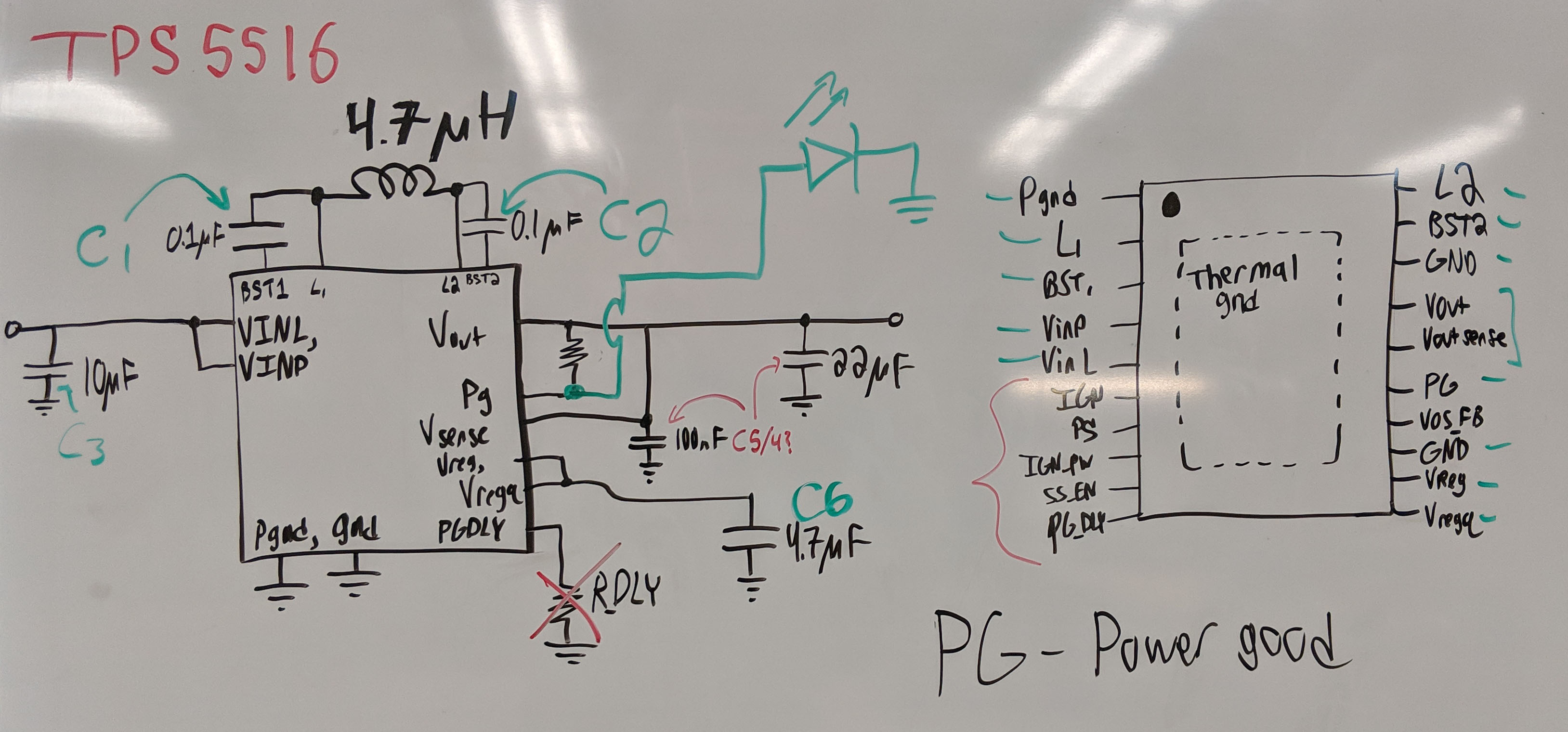
I then compared it to the printed circuit board I had on my desk, and annotated the schematic. I probed around with a multimeter. On some of the boards I was getting some odd readings, the V_Sense and V_Reg pins were reading the 5V but then the V_Out was reading 2.9V. The PG pin wasn’t on, so the power indicator light was off. PG ended up standing for “Power Good”
Probing around more, all of the other components were reading fine. I then decided to look under our microscope to see if I could find anything that was wrong with the soldering job. Immediately I was greeted with two mistakes notorious with SMD work.
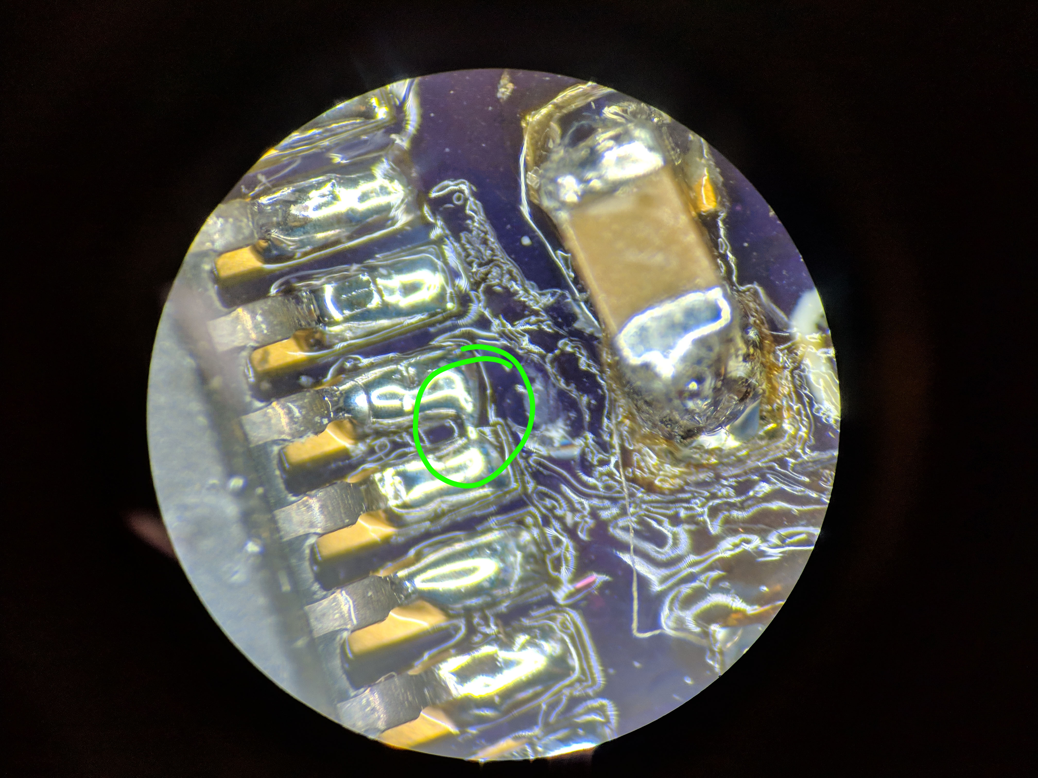
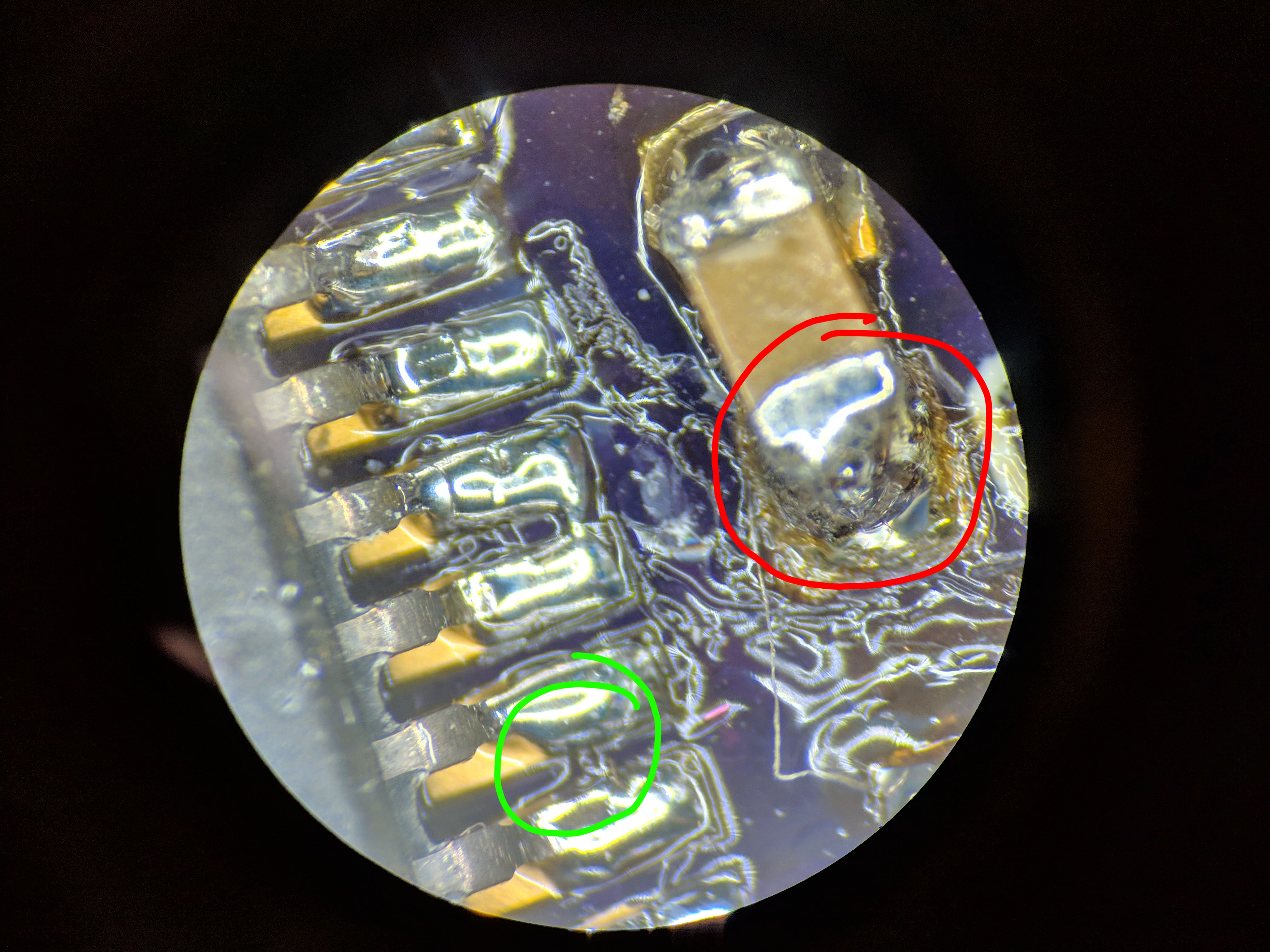
So, pins were bridged on just about every faulty board. In addition, on half of these boards, the capacitor that controls the oscillation for the buck converter wasn’t even making contact!
After cleaning up the solder jobs and cleaning the flux off the board with isopropyl alcohol, I was able to restore 9 out of 10 boards back to working order! The 10th board had a trace that was ripped off from thermal stress when the high-schoolers were soldering the large inductors on.
We were then able to package and ship them out, just in time for the Engineering without Borders team to take them to the airport.